
Learn more about how Trevisan’s Horizontal Machining Centers can help you minimize set up time and labor costs.

Top EV Charging Module PCB Design Manufacturers in China

EV Charging Module PCB Design is where electrical performance meets manufacturing discipline. A charging module may look compact, yet its board must manage heat, switching noise, high current, and limited space. On a production line, a small layout weakness can become a hot connector, unstable signal, or costly redesign. Details matter.

A useful paraphrase of power-electronics professor Robert Erickson’s engineering principles is: “Efficiency depends on controlling energy flow, heat, and switching behavior together.” This is an editorial paraphrase, not a verbatim quotation. It captures why PCB selection should go beyond a supplier’s catalog. Buyers should examine high-current layout experience, thermal design methods, material choices, fabrication tolerances, and the manufacturer’s ability to support testing and revisions. Ask to see relevant project evidence. Verify the details.

China has a broad supplier base, but capabilities vary. Some manufacturers excel at rapid prototyping; others offer stronger engineering support or volume production. This guide introduces leading Chinese manufacturers involved in EV Charging Module PCB Design and offers practical points for comparing them. Look closely at engineering communication, traceability, and how clearly a supplier explains design trade-offs. A polished presentation is not proof of a robust board. Nor is the lowest quote. No design is perfect; thermal assumptions and real operating conditions still need careful review. The right partner is the one that can explain its decisions, document its process, and improve the design when test results expose a weakness.
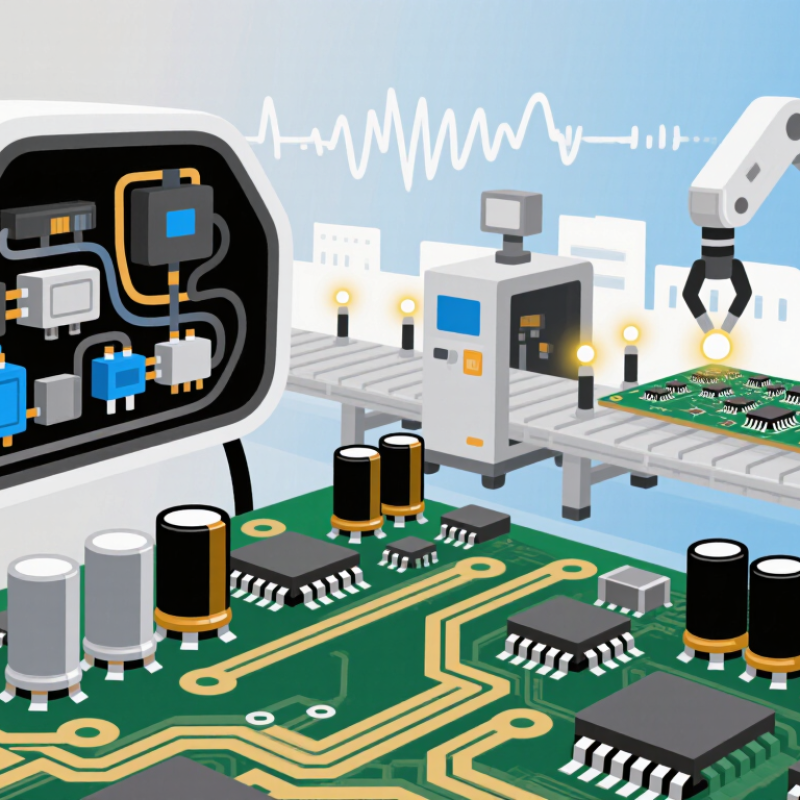
Top EV Charging Module PCB Design Manufacturers in China

What Is an EV Charging Module PCB?

What Is an EV Charging Module PCB?

An EV charging module PCB is the circuit board that links power components and control electronics inside a charging unit. In a DC fast-charging module, it may support power-factor correction, DC-to-DC conversion, gate drivers, sensing, and control. High-current copper paths, isolation gaps, and heat-spreading features matter. The PCB does not make power safe by itself. It works with the enclosure, components, firmware, and protection systems. Details vary by charger design.

The IEA’s Global EV Outlook 2024 reports more than 3 million public charging points worldwide by the end of 2023, up about 40% in one year. That growth raises demand for compact, serviceable power modules. Engineers must check creepage and clearance, copper thickness, connector temperature, and performance under load—not only schematic correctness. A small hotspot near a switching device can shorten component life. Not every layout behaves as expected.

Tips: Ask for thermal images and insulation-test results from a representative operating load. Confirm the board’s voltage, current, and cooling assumptions match the finished module. Keep measurement records. A neat layout can still run hot.

Key Design Requirements for EV Charging Module PCBs

An EV charging module PCB must carry substantial current while controlling heat, noise, and electrical isolation. Start with power-path geometry: keep high-current loops compact, use appropriately sized copper, and avoid narrow necks near connectors. Separate high-voltage switching areas from sensing and communication circuits, with clear boundaries and carefully planned isolation distances. Those distances should reflect working voltage, contamination risk, materials, and applicable safety requirements.

The switching node deserves special attention. Fast edges can couple noise into nearby signals, even when the schematic looks clean. Place gate-drive components close to their switches, and give sensitive measurements quiet return paths. Add thermal vias beneath hot components, then confirm copper planes can spread heat without compromising isolation. Trade-offs remain.

Choose laminate and copper finishes for temperature, voltage stress, and assembly process—not habit alone. Include test points for critical rails, current sensing, and communication lines; inaccessible nodes slow fault finding. Before release, ask the manufacturer to review the stack-up, impedance needs, solder-mask limits, and fabrication details. Prototype testing should check temperature rise, switching noise, and load behavior under realistic conditions. A small reroute may still be needed.

Top EV Charging Module PCB Design Manufacturers in China - Key Design Requirements for EV Charging Module PCBs
Design Area Key PCB Requirement Practical Design Considerations Relevant Reference
Voltage and insulation Define insulation distances from the actual working voltage, transient overvoltage, pollution degree, material group, and equipment installation conditions. Keep high-voltage and SELV/control circuits appropriately separated. Specify creepage and clearance requirements on drawings, and verify them on the finished PCB and assembly. IEC 60664-1; applicable EVSE product standards and regional requirements
Charging equipment safety Design the module as part of the complete charging system, not as an isolated PCB. Consider protective earthing, electric-shock protection, abnormal operating conditions, temperature rise, and coordination with enclosure, connectors, fuses, and contactors. IEC 61851-1; IEC 61851-23 for DC EV supply equipment
Power and current paths Size copper, planes, vias, terminals, and busbar interfaces for continuous and transient current under the real thermal conditions. Use current-carrying calculations and thermal measurements. Account for copper thickness, trace geometry, ambient temperature, airflow, and nearby heat sources; do not rely on trace width alone. IPC-2152; manufacturer process and component limits
Thermal management Provide a defined heat-flow path for switching devices, magnetic components, rectifiers, and other high-loss parts. Place heat-generating components with heatsink and airflow requirements in mind. Validate hot spots under full-load and worst-case ambient conditions, including enclosure effects. Thermal simulation and prototype testing; component datasheet limits
Power conversion and EMI Control switching-current loops and high-frequency noise through careful placement, routing, and return-path design. Minimize critical switching loops, keep gate-drive paths short, separate noisy power sections from sensitive sensing and communication circuits, and plan filtering and shielding interfaces early. Applicable EMC requirements; IEC 61851 series where relevant
Sensing and control Protect measurement and control circuits from power-stage noise and electrical transients. Route voltage and current sensing as controlled, low-noise paths; use appropriate isolation components and protection circuits; verify signal accuracy during switching and fault conditions. System safety analysis; isolation-component datasheets
PCB materials and construction Select laminate, copper weight, layer stack-up, and board thickness to meet electrical, thermal, mechanical, and manufacturing needs. Confirm material ratings, finished copper requirements, via construction, solder-mask clearances, and fabrication tolerances with the PCB fabricator before release. IPC-2221 for generic PCB design guidance; fabricator capability documentation
Reliability and verification Build inspection and testing into the design and manufacturing plan. Provide test access where practical. Define checks for shorts, opens, polarity, isolation, functional operation, and thermal performance; establish acceptance criteria for the assembled board. IPC-A-610 assembly acceptability; product-specific validation plan

Design values and compliance requirements depend on the charger architecture, rated voltage and power, installation environment, target market, and applicable editions of the standards. Confirm final requirements through engineering review, testing, and certification assessment.

How Chinese Manufacturers Design and Produce Charging PCBs

Top EV Charging Module PCB Design Manufacturers in China

Chinese manufacturers typically begin charging PCB design by translating module requirements into electrical and thermal limits. Engineers review operating voltage, current, switching frequency, isolation needs, and enclosure dimensions. These details guide component selection, copper thickness, layer count, and spacing. High-current paths need careful routing; a narrow trace can create excess heat. Teams may use thermal simulations, then check hot spots with sensors during prototype testing. Results matter. A model cannot capture every real-world condition.

After layout review, production teams check whether the board can be assembled consistently. They assess component clearance, solder-pad geometry, and panel layout before fabrication. Prototype boards can reveal issues such as connector stress, electromagnetic interference, or unexpected heating near power devices. Manufacturers then refine the design and run functional tests under defined loads. Inspection may include automated optical checks and tests of insulation or temperature, depending on the product requirements. One weak point is rushed iteration: a board may pass a brief test but behave differently after repeated load cycles. That deserves more attention.

Tips: Ask for test conditions, not just pass results. Confirm the PCB material, copper thickness, and temperature limits in writing. Request prototype data from realistic operating loads, and review any design changes before mass production. Small details matter.

Copper Weight and Approximate Thickness for Charging PCBs

Copper weight is one factor manufacturers consider when designing high-current charging circuit boards. The chart shows the approximate thickness conversion: 1 oz/ft² of copper is about 34.8 μm. Actual copper selection depends on current, temperature rise, trace geometry, and the full PCB stack-up.

Leading EV Charging Module PCB Manufacturers in China

Leading EV charging module PCB manufacturers in China are evaluated on more than board price. Their work must support high current, heat, and continuous operation inside compact power modules. The IEA’s Global EV Outlook 2024 reports that public charging points worldwide grew by 40% in 2023, while fast chargers grew by 55%. This expansion increases demand for robust power-conversion hardware. Small details matter. Buyers should check copper weight, insulation performance, thermal management, and trace spacing against the module’s actual voltage and current requirements.

Strong manufacturers provide engineering support before production begins. They review Gerber files, flag tight clearances, and discuss heat paths around power components. Ask for production samples, cross-section images, and test records—not only a capability sheet. Traceability and controlled process changes also matter when boards move from prototype to volume. A datasheet cannot reveal every production variation. Still, no audit captures everything, and suppliers may need to refine processes after initial builds. Clear communication about defects and corrective actions is therefore a useful sign of manufacturing maturity. These checks help distinguish a capable PCB partner from a low-cost supplier whose board performs well only under ideal conditions.

How to Evaluate and Select a Chinese Manufacturer

Selecting a Chinese EV charging module PCB manufacturer requires more than comparing quotations. The IEA’s Global EV Outlook 2024 reports that China held about 70% of the world’s public charging points in 2023, including roughly 85% of fast chargers. That scale makes local production capacity attractive, but it does not prove a factory can build reliable high-power boards. Ask for process records covering copper thickness, laminate selection, soldering, and electrical testing. Specific evidence matters.

Review the manufacturer’s experience with high-current layouts and thermal management. Request sample cross-sections, impedance results where relevant, and temperature-rise data from loaded boards. Check how the team controls creepage distances, insulation, and component placement around heat-generating devices. Ask to see traceability from incoming materials to finished assemblies. A tidy presentation is not enough. Verify it.

A site audit should include calibration records, failure-analysis examples, and corrective-action reports—not just a guided tour. Ask how the supplier handles design changes, component shortages, and repeat defects. Compare pilot-run results with the approved design files, then review production yield and test coverage. I would also ask for a small trial build; it can reveal communication gaps that a polished audit misses. One detail is easy to overlook: confirm who owns test fixtures and process documentation if production later moves.

Scroll to Top
Scroll to Top